Tag: Analog-to-Digital

MCP3008 with Raspberry Pi

MCP3008 with Raspberry Pi

Since the Raspberry Pi is fundamentally a digital device, any I/O that is done through it’s GPIO pins will happen through high (one) and low (zero) states. When it comes to input signals that are analog, most likely from a transducer, they need to be converted to the digital domain so the Raspberry Pi can understand them. The MCP3008 is a 10-bit 8-channel analog-to-digital converter chip that has a very straightforward API implementation in GPIO Zero. The MCP3008 device uses an SPI (Serial Peripheral Interface) communication protocol that is fully taken care by the API.

SPI requires four pins for the communication:

  • A “SCLK” pin which provides the clock (pulse train) for the communication.
  • A “MOSI” pin (Master Out, Slave In) which the Pi uses to send information to the device.
  • A “MISO” pin (Master In, Slave Out) which the Pi uses to receive information from the device.
  • A “CEX” pin which is used to start and end the communication with the device, usually for one data sample at a time. Because the Raspberry Pi can have more than one device sharing the same SCLK, MOSI, and MISO pins, the CE0 or CE1 pin will indicate which device to use.

Additionally, the MCP3008 requires two separate voltage inputs ranging from 2.7 to 5.5V. The supply voltage at 5V allows for a higher data sampling rate of 200 kSamples/s (which should be plenty for the Raspberry Pi). A reference voltage of 3.3V improves the absolute resolution to about 3 mV instead of 5 mV since, for a 10-bit device, 1LSB = VREF/1024. However, the choice of VREF also has to satisfy the analog input range requirement of the transducer. If the input is higher that 5V, a resistive voltage divider can be used. Finally, in the case of a Raspberry Pi, both the digital and analog grounds on the device can share the same GND pin.

Important! You must enable the SPI for the MCP3008 communication to work. To do so, go to the Raspberry Pi Configuration menu and select Enable for the SPI in the Interfaces tab.

Hardware vs. Software SPI implementation

The Raspberry Pi has both a hardware and a software implementation of the SPI protocol. It is worth investigating what kind of sampling rates can be achieved with those two types.

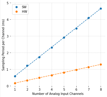
The figure on the left shows a comparison between software and hardware implementation results of the sampling period per channel as a function of the number of analog inputs. The code used to collect the data, as well as GPIO pin configurations, can be found on my GitHub page.

For each point on the graph, data was sampled as fast as possible, i.e., with no time step clock, where the only I/O occurring in the execution loop was reading the MCP3008 output. Computational time storing the data in an array was negligible. Not surprisingly, the sampling period increases linearly with the number of input channels and, on my Raspberry Pi 4B, the hardware implementation is in average 3.6 times faster than the software one.

The hardware sampling rate is approximately 6.25 kSamples/s and the software one is approximately 1.72 kSamples/s. Note that it’s common to use Samples (or kSamples) per second for a DAQ device, where the number usually gives the maximum throughput of the device. For example, 5 channels with the hardware implementation still gives 6.25 kSamples/s. However the rate is 1.25 kSamples/s per channel.

Still on the 5 channels example, you can very likely get away without an anti-aliasing filter. Noise above 625 Hz (half of the 1250 Hz sampling rate) should have negligible amplitude and shouldn’t show up as an alias in the actual signal. That doesn’t mean that the analog signal being collected with the MCP3008 doesn’t have (relatively) low frequency noise, which in turn can be filtered using a digital low-pass filter in the DAQ software.

Example with a Potentiometer

A potentiometer is basically a variable resistive voltage divider that will output a voltage between a high and a low voltage value, in our case VREF and GND. Because potentiometers convert a linear or angular position input to a voltage output, they do fall into the transducer category.

In this example, the analog output of the potentiometer will be sampled by the DAQ software. To add a bit of visual excitement, the sampled voltage will be used to change the PWM output that controls the intensity of the LED.

The wires on the right hand side of the figure are all connected to the appropriate pins on the Raspberry Pi. Since hardware SPI will be used:

  • SCLK = GPIO11
  • MISO = GPIO9
  • MOSI = GPIO10
  • CEO = GPIO8

PWM is connected to GPIO16. Note that the LED requires a series resistor, where R can be anywhere between 300 to 1000 Ohm.

Also, pay attention to the semi-circular notch on the MCP3008 chip, so it can be inserted with the right orientation into the breadboard.

The Python code for the example is shown below, where there are a few things worth mentioning:

  • The sampling period is 0.02 s, which gives a sampling rate of 50 Samples/s. That is far below the limit for the hardware SPI implementation (6.25 kSamples/s) and even the software one (1.72 kSamples/s).
  • The execution loop concept with a time step clock is used to ensure a fairly accurate sampling period. Both I/O and computation tasks are performed within a time step with plenty of time to spare.
  • Due to the noise in the analog signal, most likely due to the questionable quality of the potentiometer, a digital low-pass filter is implemented in the code. The cutoff frequency of 2 Hz can be modified for some extra exploration of its effect.
  • For the plotting of the sampled signal to work, a module named utils.py has to be accessible for importing as discussed in my previous post A useful Python plotting module.
import time
import numpy as np
from utils import plot_line
from gpiozero import PWMOutputDevice, MCP3008

# Creating LED PWM object
led = PWMOutputDevice(16)
# Creating ADC channel object
pot = MCP3008(channel=0, clock_pin=11, mosi_pin=10, miso_pin=9, select_pin=8)
# Assining some parameters
tsample = 0.02  # Sampling period for code execution (s)
tstop = 10  # Total execution time (s)
vref = 3.3  # Reference voltage for MCP3008
# Preallocating output arrays for plotting
t = []  # Time (s)
v = []  # Potentiometer voltage output value (V)
vfilt = []  # Fitlered voltage output value (V)
# First order digital low-pass filter parameters
fc = 2  # Filter cutoff frequency (Hz)
wc = 2*np.pi*fc  # Cutoff frequency (rad/s)
tau = 1/wc  # Filter time constant (s)
c0 = tsample/(tsample+tau)  # Digital filter coefficient
c1 = tau/(tsample+tau)  # Digital filter coefficient
# Initializing filter previous value
valueprev = pot.value
time.sleep(tsample)
# Initializing variables and starting main clock
tprev = 0
tcurr = 0
tstart = time.perf_counter()

# Execution loop
print('Running code for', tstop, 'seconds ...')
while tcurr <= tstop:
    # Getting current time (s)
    tcurr = time.perf_counter() - tstart
    # Doing I/O and computations every `tsample` seconds
    if (np.floor(tcurr/tsample) - np.floor(tprev/tsample)) == 1:
        # Getting potentiometer normalized voltage output
        valuecurr = pot.value
        # Filtering value
        valuefilt = c0*valuecurr + c1*valueprev
        # Calculating current raw and filtered voltage
        vcurr = vref*valuecurr
        vcurrfilt = vref*valuefilt
        # Updating LED PWM output
        led.value = valuefilt
        # Updating output arrays
        t.append(tcurr)
        v.append(vcurr)
        vfilt.append(vcurrfilt)
        # Updating previous filtered value
        valueprev = valuefilt
    # Updating previous time value
    tprev = tcurr

print('Done.')
# Releasing pins
pot.close()
led.close()
# Plotting results
plot_line([t]*2, [v, vfilt], yname='Pot Output (V)', legend=['Raw', 'Filtered'])
plot_line([t[1::]], [1000*np.diff(t)], yname='Sampling Period (ms)')

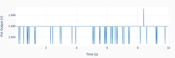
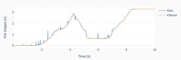
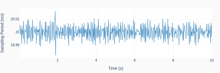
The graphs below show the results of one run on my Raspberry Pi 4B. Observe how the low-pass filter removes the noise from the raw signal as I twirl around the potentiometer knob. That of course comes with a price: the filtered signal now lags the original signal. In DAQ applications where the signal doesn’t need to be filtered in real-time, there are “zero-lag” filtering techniques that can be applied after the signal was acquired. Also note the consistent sampling time step of 20 ms.

A note on Quantization

What would happen if I never touched the potentiometer during the program execution, leaving its output at a constant value? The result is shown in the next graph, where the quantization effect is quite clear on the (very low amplitude) signal noise riding on top of the output voltage. The discrete nature of the output can now be observed, and the values are exactly VREF/210 = 3.3/1024 = 0.0032 V apart!

Analog-to-Digital Conversion

Analog-to-Digital Conversion

Also known as ADC, is the process of converting a physical quantity, usually represented by a voltage at this point, to a set of bits that’s more suitable for a computer to digest. Bearing in mind that the world we live in is analog in nature and the computers we use to interact with it are digital, going from the continuous domain to the discrete domain is an integral part of most machines and devices out there.

Back in the day, when micro-processors and computers weren’t around or were still in their infancy, many systems would function entirely in the analog domain. Take for instance an old record player. From the needle running in the record tracks (a continuous profile of peaks and valleys) to the sound coming out of the speakers, the entire sequence of changes in physical quantities occurred in the analog domain. Nowadays, still on the same example, music is stored as digital content and only converted back to an analog signal when it’s time to make it to the speakers, so we can listen to it with our good old analog ears. This last process of going back from the discrete to the analog domain is handled through a digital-to-analog conversion (DAC) and will be a topic of another post. The entire process can be illustrated with the diagram below.

As I alluded to at the very top, a sensor (or more specifically a transducer) will convert the measured physical quantity to an electrical signal, and ultimately a voltage. The next step in the process is the signal conditioning where some sort of filtering will be applied to the measured voltage. Not only to avoid aliasing, which we will discuss later on, but some times to accomplish other goals, like for example remove a DC component or a very slow drift in the signal.

The next block is the analog-to-digital conversion (ADC), which has mainly two tasks to it: sampling and quantization. Once they are performed, the continuous signal will be broken down into packets of bits that the computer can now handle. We will see that the signal is not only discrete in time but also each sample can only have a finite number of values.

At the bottom half of the diagram is the flip side of the coin: the digital-to-analog (DAC) conversion, an eventual power amplification and, generally speaking, the electro-mechanical actuators.

You should also note that if we are talking about data acquisition only, the focus is the top half of the diagram. If automation is the case, then the entire diagram is in scope.

Sampling

A physical system changes its states continuously over time and it would be impractical to collect continuous data to be used by an inherently discrete system such as the computer. Using the music example, and going back several decades, data would be collected and recorded on magnetic tapes so it could be later edited, mixed, and reproduced. With the computer entering the landscape, those analog systems had their days numbered.

The sampling process occurs in an integrated circuit (IC), where an electronic switch will bring a sample of the signal into the AD converter at a fixed sampling period.

The figure on the right shows 2 seconds of an arbitrary continuous signal sampled at 0.1 seconds (or 10 Hz). The first thing to notice is that we can now store 20 data points instead of an impractical infinite number of continuous points.

There are other considerations that dictate the sampling period (or frequency) than just the amount of data that can be manipulated. The main one is the frequency content of the signal. In other words, how “fast” does the signal change over time. For good signal reconstruction in the time domain, a sampling rate of 10 to 20 times the frequency content of the signal should be used. Most importantly, it must never be below 2 times the highest frequency component of the measured signal. Otherwise, aliasing will potentially occur to the sampled data.

As a quick note, all the plots used in this post were generated using Python and the Matplotlib package. You can get the code on my GitHub page.

Nyquist Theorem and Aliasing

According to the Nyquist sampling theorem, the sampling rate should be at least two times the maximum frequency component of the measured signal. The figure below shows a 20 Hz sinusoidal signal sampled at 21 Hz. Any sampling rate below 40 Hz will result in an alias of the original signal. In this case a new 1 Hz sinusoidal wave will show up.

The frequency of the aliased signals (yes, there’s more than one alias) is not exactly intuitive, as it appears to be in the previous figure. The same original 20 Hz signal sampled at 7 Hz would also produce a 1 Hz aliased signal! Check out the Python code on my GitHub page for a couple of formulas and to explore different sampling rates.

In practical terms, it is hard to guarantee that the signal being sampled won’t contain stray frequencies above the Nyquist frequency. The best way to avoid aliasing is to use an analog low-pass filter before the signal is sampled. Even a simple passive RC filter should suffice, provided a reasonable frequency transition band to accommodate for the poor filter attenuation right above its cut-off frequency.

Back to the music example, audio is usually sampled at 44.1 kHz. Since the human ear can respond to frequencies up to about 20 kHz, sound should be sampled at least at 40 kHz. 44.1 kHz gives a Nyquist frequency of 22.05 kHz and therefore a transition band of 2.05 kHz for a filter with a cut-off frequency of 20 kHz. However, it’s not uncommon to record audio at 48 kHz (or even 96 kHz). The former gives a Nyquist frequency of 24 kHz and therefore a wider 4 kHz transition band for a low-pass filter to attenuate the signal above it’s cut-off frequency of 20 kHz.

For the classically inclined, how does 48 kHz compare with the frequency contents of the music that’s being recorded? A soprano can hit C6 (1046.5 Hz), a violin A7 (3520 Hz), and a piano C8 (4186.01 Hz). Those frequencies are well bellow the Nyquist frequency of 24 kHz and even 10 times (or more) lower than the 48 kHz sampling frequency, allowing also for good signal reconstruction in the time domain.

Quantization

The second task in the AD processing is the quantization of the sampled values. Even though your computer can deal with floating numbers (they’re still a bunch of bits in disguise), the ADC device still ships out a packet of bits for every analog sample. The analog value will be discretized based on a reference voltage and the number of bits used for the quantization.

The ideal transfer function (TF) between the analog input voltage and the digital output code is a straight line where for every possible input there’s a unique output. In other words, the ideal ADC has an infinite resolution. Because the output of the conversion is a digital value, the transfer function of a perfect ADC is in fact a staircase function where each step is 1 LSB (Least Significant Bit).

As shown in the figure, let’s consider the case with a reference voltage VREF = 2 V and a resolution of 3 bits. The step size (1 LSB) is 0.25 V, or in the general case VREF / 2n, where n is the number of bits of the ADC.

Any analog input within a step will be coded to the same digital output. For example, 0.625 to 0.875 V will be coded as 011 (or 3 in decimal representation). Using the reference voltage of 2 V, that would give us 3VREF / 8 = 0.75 V. Therefore, the quantization error goes from +0.125 V to -0.125 V. In other words +/- 0.5 LSB. This would be the case for the perfect ADC shown in the figure, more specifically a single-ended mode configuration with adjusted quantization. A good source explaining other configurations and also sources of errors that occur on an actual ADC can be found here. The full scale (FS in the figure) is VREF – 1LSB, which in the case of this example would be 1.75 V.

If a 4-bit converter is used, the quantization error for the same reference voltage drops to +/- 0.0625 V (still +/- 0.5 LSB) and the FS goes up to 1.875 V.

As we move up in bit resolution, the ADC output starts to approximate the ideal transfer function. In the case of a 10-bit ADC, the quantization error becomes +/- 0.5VREF/1024. Which in our case is approximately +/- 0.001 V, and in the general case +/- 0.05 % of the reference voltage. For a high accuracy 16-bit ADC, the error is approx. +/- 0.0008 % of the reference voltage.

Note that there are additional errors introduced in the quantization process due to offsets, non-linearities, and just noise in general in the electronic circuitry. A 12-bit converter will typically have +/- 0.13 % (instead of +/- 0.012 %) and a 16-bit a typical +/- 0.01%.

Practical Considerations

So, how high should you go with the sampling rate and number of quantization bits? How about the anti-aliasing filter? Keep in mind that faster, higher-resolution hardware comes with a steeper cost. And high sampling rates bring the burden of extra storage space and processing power.

If you are working with audio, definitely 48 kHz and 16-bit ADC for sound recording. 96 kHz (or even 172 kHz) and 24-bit if you’re a pro. And most definitely an anti-alias filter. By the way, the fact that 96 kHz is two times the 48 kHz base rate makes it very easy to down sample a recording for later reproduction: just throw away every other data point.

If you’re toying around with a Raspberry Pi, the sampling rate is the one that suits your needs. For slow changing temperatures 1 Hz is plenty. Pressures maybe 10 to 20 Hz. A 10-bit ADC MCP3008 chip is inexpensive and has plenty of resolution. An anti-aliasing filter is probably overkill. The higher frequency content of noise is also usually low amplitude and therefore shouldn’t affect you signal very much. However, it’s always a good idea to sample your data first at a higher frequency and inspect it as a function of time. Also, be careful with some typical electrical noise like the 60 Hz one caused by the AC outlet.

In a lab or instrumentation setting, 12 to 16-bit and an anti-aliasing filter, such as a simple passive RC one, should be considered. Again, try different sampling rates and filters. As I mentioned before, it’s always important to look at your data as a function of time first with as high as a sampling rate that can be run with the DAQ device at hand. Once you understand what the signal is all about, then a more conscious decision about the hardware requirements can be made.

Finally, just to have some fun with Python, below is the arbitrary signal of this post with two different sampling rates and resolutions. Observe the effects of both the sampling and the quantization on the original signal.