As the counterpart of analog-to-digital conversion, DAC will take a digital signal and convert it to an analog one. Paraphrasing what I mentioned in previous posts, ADC and DAC walk hand-in-hand bridging the gap between the continuous and discrete domains that modern machines and devices have to deal with.
Even though there are several types of DACs, I will talk about the PWM-based one, where a reference input voltage is switched (in the form of a digital train of pulses) into a low-pass analog filter, producing an analog output. Before we get there, let’s first talk about Pulse Width Modulation, a very clever way to go from the discrete to the continuous domain, invented in the mid-seventies. A PWM signal has two main characteristics: its frequency and its duty cycle.
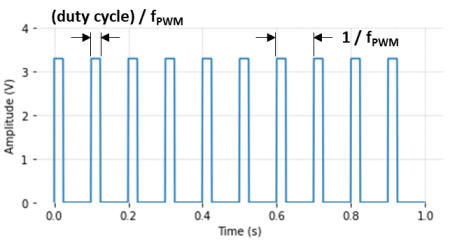
The figure illustrates the frequency and the concept of duty cycle for a 10 Hz PWM signal. In this case, the period of the PWM is 1/fPWM = 0.1 s. The chosen duty cycle is 25 %, which corresponds to the time the output is “on” (0.025 s). During the remainder of the duration of the PWM period (0.075 s) the output is “off”. As a matter of fact, it’s the modulation of the duty cycle that will control the output level of the DAC system.
Since it’s either fully “on” or fully “off”, the PWM signal is fundamentally a digital one. It’s the frequency and duty cycle of that “on-off” train of pulses, coupled with the response of the sub-system it’s interacting with, that will result in an analog behavior of the output of the overall system, in our case the digital-to-analog converter.
As a side note, the Python code used to generate the graphs in this post can be found on my GitHub page. Make sure to check it out and experiment with the DAC parameters.

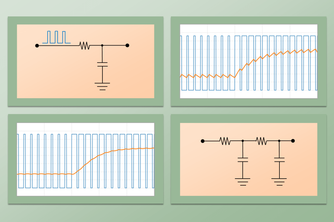
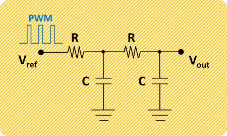
The simplest DAC implementation is shown on the left. It consists of a low-pass first-order passive RC filter connected to the PWM output signal Vref. Typically, for a TTL circuit, the voltage can be either 0 (low) or 3.3V (high).
The cutoff frequency (rad/s) of the filter is fc = 1/(RC). Along with the PWM frequency, it can be used to obtain the desired behavior of this simple DAC.
Output Ripple
The PWM signal can be thought as a sequence of low-to-high and high-to-low step inputs into the RC filter. Even with a constantly switching input, this first order system will eventually produce a near constant output. The figures below show the effect of the RC filter cutoff frequency fc as well as the PWM frequency fPWM on the amplitude of the output ripple.
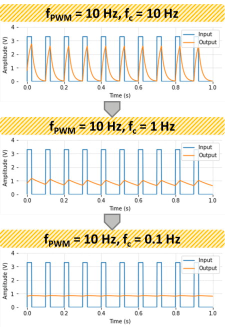

As it can be observed in the plots above, the output voltage will converge to (duty cycle) x Vref , which for the duty cycle of 25 % (used in the example) produces an output of 0.825 V when Vref = 3.3 V. Also, reducing the filter cutoff frequency or increasing the PWM frequency are both effective in reducing the output signal ripple. While having a slow RC filter can greatly reduce the ripple, that will negatively affect the DAC response time when it’s subject to a change in the desired output value.
DAC Step Response
In the case of our DAC, its response time is essentially the response time of the RC filter, i.e. 1/fc = RC (with fc in rad/s). Leaving the details for a future post on analog and digital filtering, for the first order system under consideration, the response time can be defined as the time it takes for the output to reach about 63 % of its final (steady-state) value, after a step input is applied.
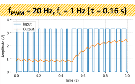
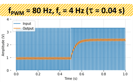
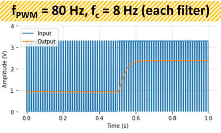
The next figure shows how an appropriate combination of a higher PWM frequency and a higher filter cutoff frequency can produce a faster response time, while maintaining roughly the same amplitude of the DAC output ripple. For our example, the response time based on the RC value goes from 0.16 s down to 0.04 s.
Cascaded Filters
The output ripple can be further improved by cascading two first-order RC filters, as shown below. The newly formed second-order filter will have twice the attenuation (dB/decade) above the cutoff frequency. It’s an easy-to-do improvement which is often adopted.
Practical Considerations
Just like its ADC counterpart, DACs also have an inherent quantization in the signal. The digital PWM, generated from the microprocessor clock, has a finite resolution (duty cycle levels) given by the number of bits of the PWM. Typical resolutions range from 8 to 12 bits.
Actual PWM frequencies for DAC devices are much higher than the ones used in the examples above, which were chosen mainly to illustrate the concepts. For applications involving testing of physical systems or automation, frequencies between 500 and 2000 Hz are reasonable. In audio applications, several times the highest frequency of the audible range (20 kHz) seems to be the case. That is, 100 to 200 kHz. However, just as we observed when using higher order filtering, there’s wiggle room to reduce these numbers while still having a good compromise between response time and ripple.
It’s important to make a distinction at this point: if the PWM is used to drive a DC motor directly (or with some power amplification), the motor itself will behave approximately as a first order system. Hence, there’s no need for the RC filter. In this type of application, PWM frequencies of 100 to 200 Hz are just fine.
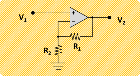
Amplification of the DAC output beyond the typical 3.3V Vref, can be achieved by using an Op Amp (Operational Amplifier). For a simple non-inverting amplifier, the output voltage is given by:
V2 = V1(1+R1/R2)
By choosing R1 = R2 = 10 kOhm, we can double the output to accommodate a more typical 0 to 5V requirement.
In my next post, we will explore the implementation of a DAC using a Raspberry Pi and a few resistors and capacitors. The Pi has hardware enabled PWM on two of its GPIO pins, which can reach frequencies in the kHz range! That should be an interesting project.
