Let’s put some of the concepts from the Digital-to-Analog Conversion post to work with a Raspberry Pi. To get the most out of it, you will need a few resistors and capacitors, as well as an MCP3008. The former will be used to build the low-pass analog filters, while the latter will be used to measure the DAC output. As a general guideline, you don’t want to generate and measure a signal on the same DAQ device, since all sorts of extraneous loops and noise could potentially show up. But because we’re not doing any instrumentation-critical work, we won’t be following that guideline.

The figure shows the layout of the components on a breadboard. The MCP3008 wires will use the same pins that were used in the MCP3008 with Raspberry Pi.
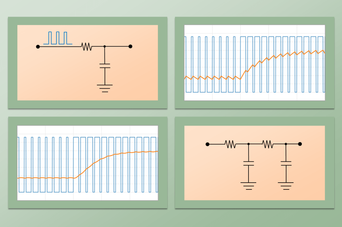
The PWM wire should be connected to GPIO12, which is one of the hardware-implemented PWMs on the Pi (GPIO13, 18, and 19 also have hardware PWM). As a side note, the software-implemented PWM is good for 100 to 200 Hz. The PWM period starts to fall apart above 500 Hz. The hardware PWM can go up to 8 kHz! However, that would be an overkill for our application and we will settle down for a lower value, as shown later on.
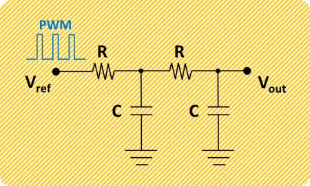
It’s also possible to identify on the board two cascaded low-pass RC filters, whose output is connected to pin 1 on the MCP3008 (channel 0 on the GPIO Zero MCP3008 class).
Let’s aim for a step response time (τ) of 0.01 s for our filters. We can then use the formula τ = RC to determine the RC product and choose suitable R and C values. In our case, we should select R = 1 kΩ and C = 10 μF. When putting everything together, make sure the negative side of the capacitors are connected to ground!
The following Python code (mostly derived from the example in Prescribed PWM duty cycle) will run a sequence of PWM duty cycle steps that can be used to better understand the DAC output. Check the list of comments below before digging into the code.
- Even though the hardware PWM can go up to 8 kHz, it seemed reasonable to use 700 Hz for it. Change this number to lower values (such as 50 Hz) to see the impact on the signal ripple.
- Both the PWM values as well as the ADC measurements are normalized between 0 and 1 in GPIO Zero. Therefore, they are scaled throughout the code to Vref = 3.3 V.
- The PWM duty cycle output steps (that correspond to a DAC output) span the entire range. However, the 0 and 1 values are omitted. That’s because they fully bypass the PWM, applying respectively a constant 0 and Vref to the output.
- Even though the sampling rate of the hardware-based ADC can go up to 6.25 kSamples/s, the signals are sampled at a rate of 500 Samples/s. That’s sufficient for visualization and provides plenty of margin in the execution loop.
import time
import numpy as np
from utils import plot_line
from gpiozero import PWMOutputDevice, MCP3008

# Assigning parameter values
pwmfreq = 700 # PWM frequency (Hz)
pwmvalue = [0.05, 0.2, 0.4, 0.6, 0.8, 0.95, 0.9, 0.7, 0.5, 0.3, 0.1]
tsample = 0.002 # Sampling period for data acquisition (s)
tstep = 0.5 # Interval between PWM output step changes (s)
tstop = tstep * len(pwmvalue) # Total execution time (s)
vref = 3.3  # Reference voltage for the PWM and MCP3008

# Preallocating output arrays for plotting
t = []  # Time (s)
dacvalue = []  # Desired DAC output
adcvalue = []  # Measured DAC output

# Creating DAC PWM and ADC channel (using hardware implementations)
dac0 = PWMOutputDevice(12, frequency=pwmfreq)
adc0 = MCP3008(channel=0, clock_pin=11, mosi_pin=10, miso_pin=9, select_pin=8)

# Initializing timers and starting main clock
tprev = 0
tcurr = 0
tstart = time.perf_counter()

# Initializing other variables used in the loop
count = 1  # PWM step counter
dacvaluecurr = pwmvalue[0]  # Initial DAC output value
dac0.value = dacvaluecurr  # Sending initial value to GPIO pin

# Running execution loop
print('Running code for', tstop, 'seconds ...')
while tcurr <= tstop:
    # Updating PWM output every `tstep` seconds
    # with values from prescribed sequence
    if (np.floor(tcurr/tstep) - np.floor(tprev/tstep)) == 1:
        dacvaluecurr = pwmvalue[count]
        dac0.value = dacvaluecurr
        count += 1
    # Acquiring digital data every `tsample` seconds
    # and appending values to output arrays
    # (values are converted from normalized to 0 to Vref)
    if (np.floor(tcurr/tsample) - np.floor(tprev/tsample)) == 1:
        t.append(tcurr)
        dacvalue.append(vref*dacvaluecurr)
        adcvalue.append(vref*adc0.value)
    # Updating previous time and getting new current time (s)
    tprev = tcurr
    tcurr = time.perf_counter() - tstart

print('Done.')
# Releasing pins
dac0.value = 0
dac0.close()
adc0.close()

# Plotting results
plot_line([t]*2, [dacvalue, adcvalue], yname='DAC Output (V)')
plot_line(t[1::], 1000*np.diff(t), yname='Sampling Period (ms)')
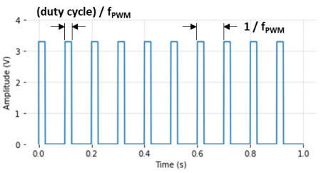
The plots show the output generated using plot_line from the utils.py module. Make sure you have a copy of it that can be imported. Observing the DAC response, it’s possible to notice that for lower PWM duty cycles the stead-state value is higher than the set point. Conversely, a higher duty cycle produces a steady-state value lower than the set point. Later on, we’ll see that it is possible to calibrate the DAC output so a one-to-one relationship can be obtained. It’s also a good practice to plot the actual sampling period that the execution loop is running on. Just to make sure it can keep up.


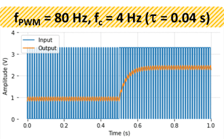
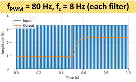
Output Ripple and Step Response
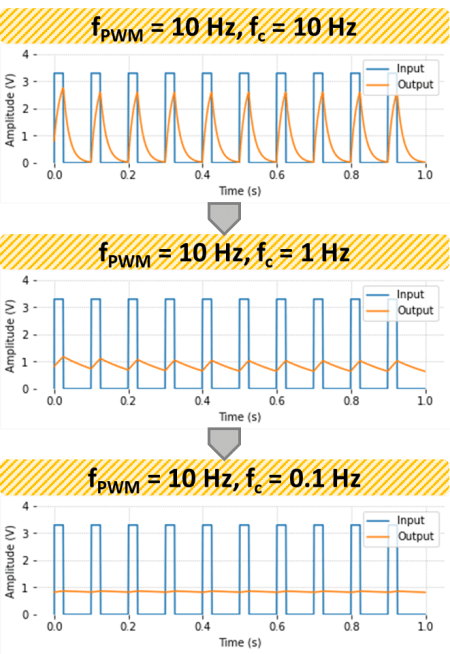
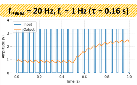
The next figures show the step response of our Pi DAC for a PWM duty cycle change from 25 to 75 % (0.825 to 2,457 V), respectively for PWM frequencies of 50 and 700 Hz.
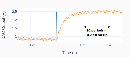
For the 50 Hz PWM, the ripple in the output is quite significant and can be easily identified. We can also see that there’s no offset between the desired and the actual steady-state DAC output signals. In the other hand, for the 700 Hz PWM, the ripple in the output is much smaller and isn’t related to the PWM frequency. Unlike the lower frequency case, there’s now an offset between desired and actual outputs.
That offset is mostly caused by the transitions from low-to-high (and vice-versa) in the PWM signal. Because they’re not instantaneous (think of them as very steep ramps instead), the PWM signal going into the low-pass filter will assume values other than low (0V) and high (Vref). These intermediate values become more relevant the higher the frequency is. Interestingly enough, the offset will be zero at 50% duty cycle, regardless of fPWM.

The response time is not affected by the PWM frequency. The theoretical value of 0.02 s (for the combined cascaded low-pass filters used in this example) wasn’t observed on the actual signal. The higher response time of 0.05 s is due in part to the PWM not being a perfectly “square” wave form. One should also speculate other delays in the Raspberry Pi hardware itself, as well as the effect of input/output impedances.
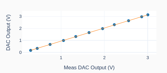
DAC Calibration
The relationship between the set point and the actual analog output values is quite linear and can be determined with the help of a modified version of the Python code above, which also performs a linear regression on the collected data. The code stores (and averages) analog output data for the steady-state portion of every step of the input sequence. The data points are then used in a linear regression to determine the transfer function between desired and actual analog output values. The graphs below show the linear regression and the calibrated output. Check out the code on my GitHub repository for more details.

Final Remarks
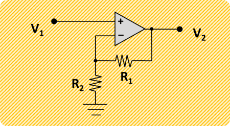
While most instrumentation and DAQs these days don’t require analog inputs to do what they’re supposed to do, some of the older pieces of equipment out there still do. Op Amps can be used to expand the output voltage range of our simple Pi DAC to a more common 0 to 5 V.
In this post, I create a DAC class that can be used like any other GPIO Zero class (such as PWMOutputDevice or MCP3008) making it much easier to work with the code. The exercise of building the class also comes in handy as we explore more efficient ways to write DAQ software in Python.